Quobly is bringing a proven semiconductor technology—FD-SOI—to quantum computing. We believe that minimally modifying existing VLSI manufacturing processes honed over decades is the best way to scale up quantum in existing semiconductor fabs. This approach will also position us to fine-tune control of our qubits by optimizing qubit design and manufacturing processes to tightly integrate qubits and standard CMOS control electronics on the same chip. Read on to learn about the advantages of FD-SOI and the hurdles to scaling up quantum on silicon—not least of which is overcoming the impacts of defects in the material.
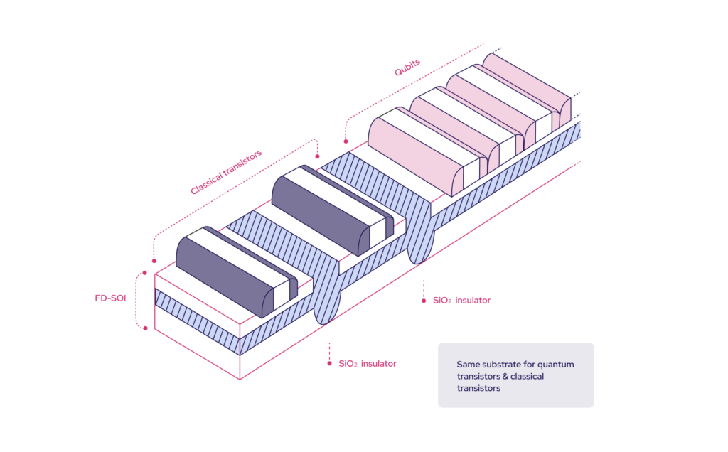
From classical transistor to qubit
Quobly is solidly anchored in the European semiconductor hub of Grenoble, France and is a spinoff of the CEA, just like FD-SOI manufacturer Soitec and Quobly partner STMicroelectronics, which has been manufacturing chips found in everything from smartphones to cars using 28 nm FD-SOI processes for decades. Today, these mature processes are reliable and their yields predictable. And we know how to characterize the electrical behavior of these chips at room temperature. However, to create qubit functions, the chips must be able to operate at very low temperatures (4 Kelvin). One of Quobly’s R&D priorities is to characterize these known chips’ very different behaviors at very low temperatures so that the existing models used to manufacture conventional transistors can be updated to manufacture our qubits and the associated cryoelectronics.
But what will VLSI manufacturing of our quantum chip look like, exactly? To bring a quantum processing unit/quantum integrated circuit (QPU/QIC), to the market at a reasonable cost and within a reasonable timeframe, modifications to existing VLSI manufacturing processes will have to be kept to a minimum. We will use the same process flow already in place at certain Tier 1 foundries, but with a few new steps to fabricate a new function—our silicon spin qubits—on these proven chips. The process modifications will be tested in the advanced R&D cleanrooms at CEA-Leti, another Quobly strategic partner.
This is a new “more Moore” CMOS scaling scenario that echoes the integration of past generations of new logic, memory, photodiode, and interconnect technologies into existing process flows to meet demand for conventional transistors from markets like high-performance computing, mobile, and IoT.
Today, Quobly is preparing to integrate qubits onto chips whose design has been optimized for quantum. The difference with past iterations of semiconductor chips is that quantum is not just a new market—it is a completely different paradigm that will offer unrivalled efficiency for specific real-world computing problems. Remember, rather than binary ones and zeroes, qubits can be in multiple states simultaneously, opening the door to new mathematical approaches that could solve currentlyintractable problems in very specific fields like materials science and chemistry, for example.
Qubit connectivity, essential for error correction
Parts of Quobly’s technology originated at CEA-Leti, a leading global center for advanced integrated circuit R&D and home to a beyond-state-of-the-art 300 mm clean room dedicated to characterization and prototyping. We continue to work with CEA-Leti to pave the way for future generations of our silicon spin qubits while we transfer our current generation to a commercial fab. This is an iterative process in which we are utilizing CEALeti’s cleanrooms to push back the limits of what is possible before scaling up each new element of our future process flow. Our strategic partnerships with Tier 1 foundries will be vital to helping us advance through our R&D roadmap as planned.
So, where does our technology currently stand? One thing is certain: There will be several generations of quantum technology, with increasing qubit connectivity from one generation to the next.
Technology focus: increasing qubit connectivity, one generation at a time
| FIRST GENERATION | Materials and processes optimized for qubits with 99.9% fidelity; limited error correction. |
| SECOND GENERATION | Higher qubit connectivity and enablement of extended error correction capabilities. |
| THIRD GENERATION+ | Multicores with quantum interconnects between cores. |
Some of our earlier-stage R&D, designed to prepare for future generations of quantum technology, is focusing on pitches under 100 nm with our R&D partner CEA-Leti, whose R&D cleanroom facilities allow us to go further in our exploration of commercially-compatible lithography for FD-SOI using iDUV. At the same time, we are scaling up our first generation at slightly larger pitches with foundries that possess solid roadmaps to smaller pitches.
Specifically, we are leveraging existing lithography processes to trap our electrons so that we can control them and get them to interact at pitches that can be achieved reliably in an industrial manufacturing scenario. As we continue to optimize design and processes, our ability to reliably control interaction between our qubits and to reduce the impacts of noise—to which qubits are notoriously sensitive—will increase. And the material from which our wafers are made plays a major role.
Enter FD-SOI, Quobly’s material of choice for quantum
As previously mentioned, optimizing the distances between electrons—pitches—is crucial to dynamically controlling the two states between two electrons (either interacting or not interacting) by applying voltage. This requires plunger gates to trap the electrons and barrier gates to control their interaction. In terms of processes, iDUV single patterning is limited at around 74 nm.
So, how do we plan to fabricate the much finer patterns needed for the barrier gates? Additional gates can be etched between previously-etched gates, requiring new masks—masks which are much cheaper at the 28 nm technology node than EUV lithography at the more advanced 5 nm, 3 nm, or 2 nm nodes that could, in theory, open the door to the finer patterns in a single process step. We currently believe that staying at less advanced nodes is the right tradeoff on the road to a manufacturable QPU.
This is where the quality of the qubit environment—the silicon—comes into play. As with conventional silicon transistors, defects in the material, due to doping, for example, create disturbances that are detrimental to qubit stability. This same capacity to trap charges is what we use—in a controlled way—to make our qubits. There are two ways to mitigate the effects of unwanted defects: finer gate pitches as discussed above, and passivation, a technique to reduce defects in the material itself, which we are working on with CEA-Leti and with materials and thin-layer deposition OEMs.
Silicon 28 provides the best environment for our qubits in terms of minimizing disturbances. French nuclear-industry stakeholder Orano is now able to purify silicon into Silicon 28 at its recently-opened largescale stable isotope facility in France, and another French corporation, Air Liquide, can transform this Silicon 28 into a gas compatible with chemical vapor deposition, a common CMOS process that we will be optimizing to make optimal use of the very expensive Silicon 28 gas. We will then have Soitec transform this substrate into FD-SOI wafers using the company’s proven Smart Cut™ process.
FD-SOI at the heart of our future manufacturing environment
Moving forward, we will continue to place FD-SOI technology at the heart of our R&D, staying at less advanced nodes to achieve the kinds of tradeoffs that have allowed conventional VLSI to reach commercial maturity and working with our local partners like STMicroelectronics to develop the modifications needed to manufacture our QPU.
Learn more about our latest scientific advances in the field of FD-SOI for quantum computing
Author
